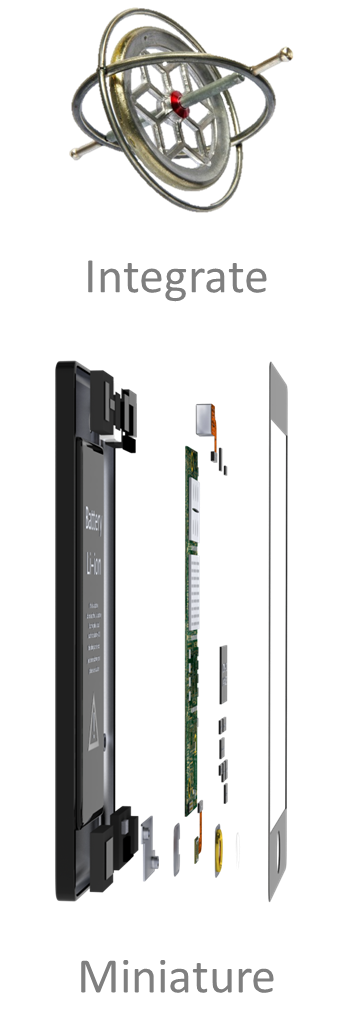
Motion Sensing Solution
MEMS Gyroscope and Accelerometer
Benefits
- Ultra-thin module height
- Small form factor (X,Y,Z)
- Performance enhancement
- Standard SMT assembly
- Enables 3D stacking
- Compatible with reflowable wafer-level cameras
- Available in both cavity and non-cavity formats, and lead and lead-free bumps format
- JEDEC Level II & III moisture sensitivity
Process
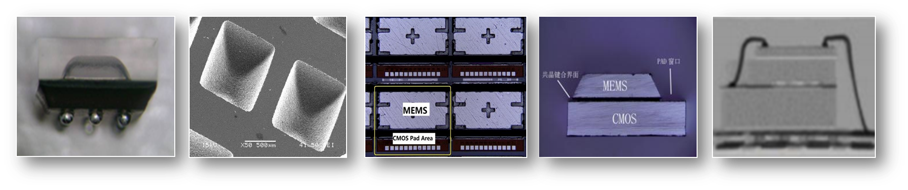
- The technology uses a breakthrough, cavity glass silicon sandwich structure that enables hermetic encapsulation of sensor. To create the structure, China WLCSP encapsulates the wafer with a hermetic cover, creates the Through Silicon Interconnects, and routes the electrical contacts, forms solder bumps on the wafer backside and singulates the wafer into an individually packaged die. This packaging process delivers small form factor and exceptionally high reliability. By ensuring the die is fully protected from enviromental condictions from the first stage, it also enhances yield for manufacturers.