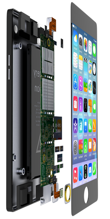
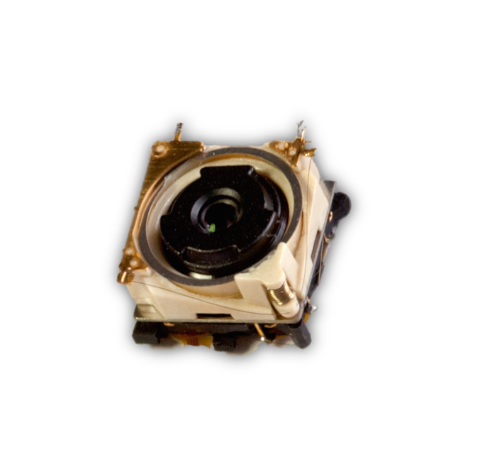
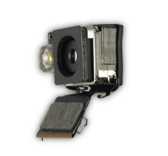
Mobile Imaging Solution
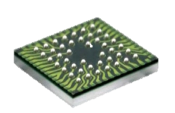
World Smallest Image Sensor Package
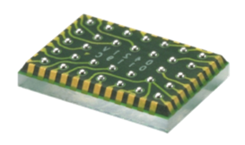
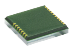
Benefits
- Ultra-thin module height
- Small form factor (X,Y,Z)
- Performance enhancement
- Standard SMT assembly
- Enables 3D stacking with ISP/DSP
- Compatible with reflowable wafer-level cameras
- Available in both cavity and non-cavity formats, and lead and lead-free bumps format
- JEDEC Level I, II & III moisture sensitivity
Process
- The technology uses a breakthrough, glass-silicon sandwich structure that enables defect-free image-sensing capabilities through the packaging. To create the structure, China WLCSP encapsulates the wafer with a glass cover, creates the Through Silicon Interconnects, and routes the electrical contacts, forms solder bumps on the wafer backside and singulates the wafer into an individually packaged die. This packaging process delivers small form factor and exceptionally high reliability. By ensuring the die is protected from contamination from the first stage, it also enhances yield for manufacturers.